Technology and application of DPC ceramic Substrate -VCSEL laser
2021-07-30 16:39:59
According to the latest global market research report, the global 5G Internet of Things market size will reach 700 million US dollars in 2020, and with the demand for iot devices and the gradual popularization of 5G technology, the market data is expected to double to 6.3 billion US dollars by 2025.
With the development and popularization of 5G Internet of Things (IOT), 3D Sensing and Sensing technology will see a rapid growth. As the core device of 3D Sensing and Sensing system, VCSEL will undoubtedly make a major breakthrough in semiconductor laser technology.
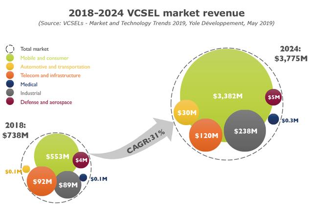
Yole expects the VCSEL market to grow from $1.247 billion in 2019 to $3.775 billion in 2024, at a compound annual growth rate of 31%. Market data unquestionably proves that VCSEL is one of the fastest growing segments of the photon market.

Credit: Yole
One, VCSEL laser
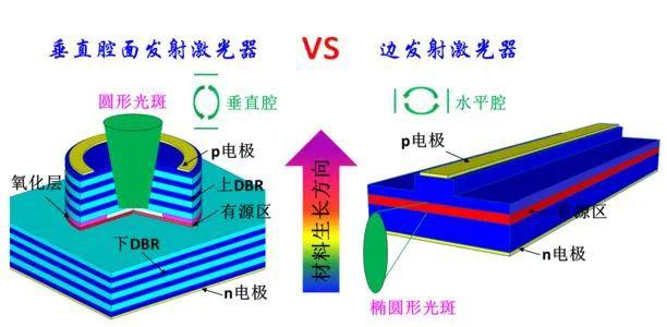
VCSEL is essentially a kind of semiconductor laser, the laser is used to launch laser device, and the semiconductor laser is a semiconductor material as the working material of the device to launch laser, according to the structure of the laser chip, the semiconductor laser can be divided into side emitting laser (EEL) and vertical cavity surface emitting laser (VCSEL).

VCSEL has the following advantages over EEL:
(1) The circular spot is easier to realize coupling with the optical fiber and the coupling efficiency is much higher
(2) Vertical light emitting is easier to achieve two-dimensional plane and photoelectric integration
(3) Low threshold current
(4) High photoelectric conversion efficiency
(5) Long service life
(6) Strong modulation ability
(7) Can be integrated with large-scale integrated circuits
(8) Without cleavage, the on-chip experiment can be carried out after encapsulation
(9) Operate in a single longitudinal mode over a wide range of temperature and current
VCSEL also demonstrates excellent performance in sensor applications, with a simpler structure, smaller volume and more accurate distance compared to the LED light sources used in earlier 3D camera systems.
Ii.VCSEL application trend
Due to the gradual growth of infrared component application market, the 3D sensing technology of terminal mobile phone, automotive optical da and optical fiber transmission are booming
1, mobile phone market support
TOF is one of the three mainstream 3D Sensing technology routes at present, the other two are binocular stereoscopic imaging and structured light. Currently, structured light and TOF are relatively mature schemes. TOF has become widely recognized in mobile terminals due to its advantages of simple structure, smaller module size, longer detection distance and lower material cost.
The working principle of TOF is that the VCSEL laser source is used as the transmitting end to emit continuous infrared light to the target, and then the infrared CIS is used as the receiving end to receive the optical signal returned by the object.
Apple already installed a "TOF optical sensor" on the rear main camera module of the iPhone 7, and the iPhone X not only continues this application, but also uses 3D structured light and TOF optical sensor components on the front face recognition module, pushing the VCSEL TOF directly to a peak.
VCSEL vendors are generally optimistic about the application prospects of ToF technology in smartphones. But in fact, 5G brings much more to the VCSEL industry.
2. The rise of the car market
With the global wave of autonomous driving and the rapid growth of "new infrastructure" proposed by the Standing Committee of the Political Bureau of the CPC Central Committee, the demand of the automotive lidar industry will undoubtedly reach a new high.
Compared with the current expensive mechanical lidar, VCSEL's solid-state lidar can better achieve the performance required by the vehicle. VCSEL's solid-state lidar has higher reliability, stability and small size, laying the foundation for large-scale application of lidar in the automotive field.
Since its birth, VCSEL has been the core device of a new generation of optical storage and optical communication applications, which is applied in optical parallel processing, optical recognition, optical interconnection system, optical storage and other fields. With the improvement of process and material technology, THE advantages of VCSEL devices in power consumption, manufacturing cost, integration, heat dissipation and other fields begin to show, and are gradually applied to commercial applications such as industrial heating, environmental monitoring, medical equipment and consumer applications such as 3D sensing.
3. VCSEL encapsulation
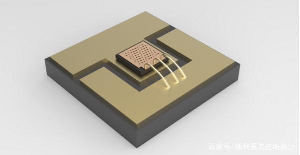
The low conversion efficiency of VCSEL chips leads to serious heat dissipation problems. To solve this problem, we need to start from the fundamental -- chip material, while the traditional circuit board FR-4 and Fe-3 are obviously unable to meet this requirement. Ceramic plates have been taking their heat dissipation performance as the main advantage. Naturally, it can well solve the problem of VCSEL's heat dissipation difference.
The power density of VCSEL is very high, and the ceramic circuit board has a high matching thermal expansion coefficient with VCSEL, so as to solve the stress problem caused by the thermal expansion mismatch between the chip and the substrate. The DPC ceramic circuit board makes the metal edge and the ceramic substrate closely combined, to avoid the later assembly process of additional sticking process, coordination accuracy and other problems, and glue aging caused by the reliability of the problem.
VCSEL structure is vertical structure, DPC ceramic circuit board has a unique high resolution, high flatness and high reliability of vertical interconnection technology advantages more suitable for its vertical eutectic welding, eliminate LTCC, HTCC thick film substrate size accuracy is not high, line rough rub and other defects.
VCSEL is above need to lens mounted to the chip, namely the substrate is the need to make 3 d chamber, Yuanxuci ceramic circuit board not only can make a planar circuit board was able to make 3 d circuit board - DAMS product, its material are inorganic ceramic materials, thermal expansion coefficient of the match, does not appear to be in the process of preparation of layer, the phenomenon such as warping.

The ceramic circuit board of DPC film technology almost meets the packaging requirements of VCSEL. Yuanxuci DPC ceramic circuit board, also known as direct copper plated ceramic circuit board, mainly with evaporation, magnetron sputtering and other surface deposition process substrate surface metallization, first in vacuum conditions sputtering titanium and then sputtering copper particles, then electroplating thickening, in the film metallized ceramic plate using image transfer mode production line, Then the high density ceramic circuit board between two - sided wiring is formed by electroplating sealing technology.
DPC ceramic substrate with high thermal conductivity, high insulation, high line accuracy, high surface flatness and thermal expansion coefficient matching chip and many other characteristics, in the high power VCSEL components quickly occupied an important position.
Iv. VCSEL -- Foreseeable future
The rapid development and unique advantages of VCSEL have made it a key device in optoelectronic applications and have strong vitality. In recent years, VCSEL with excellent performance has been continuously researched and developed, mainly involving its low threshold current, high output power, high electro-optical conversion efficiency, low working voltage, high modulation bandwidth and high yield.
It is believed that under the demand of 3D sensing, 5G communication and other fields, and the r&d investment and experience accumulation of various manufacturers, the global use of ceramic circuit board packaging VCSEL chip will make great progress, and expand more and more application fields.

