Process and application of alumina nitride on DPC ceramic substrate
2021-08-19 10:37:13
In the process of electronic packaging, the substrate mainly plays the role of mechanical support protection and electrical interconnection (insulation). With the development of electronic packaging technology towards miniaturization, high density, multi-function and high reliability, the power density of electronic system increases, and the heat dissipation problem becomes more and more serious. Good heat dissipation of devices depends on optimized heat dissipation structure design, packaging material selection (thermal interface material and heat dissipation substrate) and packaging manufacturing process, etc. Among them, the selection of substrate material is the key link, which directly affects the cost, performance and reliability of the device.
Ceramic substrate, good thermal conductivity, heat resistance, insulation, low thermal expansion coefficient and continuously reduce costs, in electronic packaging, especially in power electronic devices such as IGBT (insulated gate bipolar transistor), LD (laser diode), high power LED (light emitting diode), CPV (focusing photovoltaic) encapsulates the application more and more widely.
The preparation process of electroplated ceramic substrate includes the advantages and disadvantages of semiconductor micromachining technology, laser drilling and electroplating filling technology, electroplating growth control line and grinding, low temperature preparation process and so on. The bonding strength of metal circuit layer and ceramic substrate and electroplating hole filling are the key to the reliability of ceramic substrate and the key technology of preparing ceramic substrate.
Preparation and characteristics of electroplated ceramic substrate
From the structure and production process, ceramic substrate can be divided into HTCC, LTCC, TFC, DBC, DPC and so on. Electroplated ceramic substrate (DPC) is made by thin film process on ceramic substrate. It has stable chemical properties, high thermal conductivity, fine circuit and thermal expansion coefficient (CTE) matching with chip materials. Therefore, it has become an important development direction of high power LED encapsulation and heat dissipation substrate.
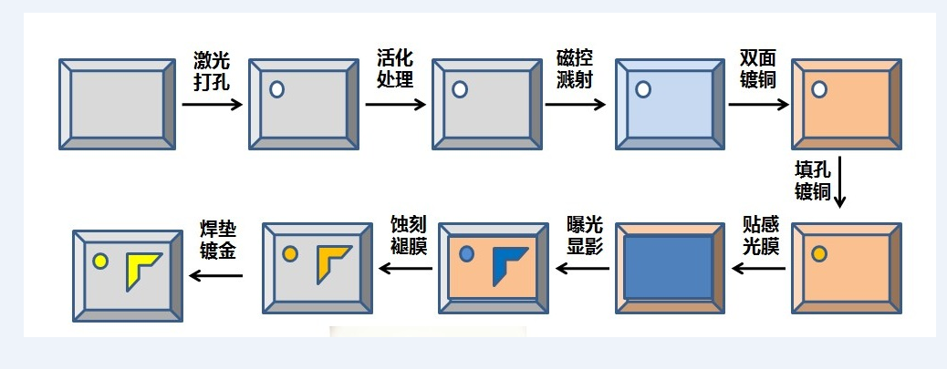
The preparation process of DPC ceramic substrate is shown in Figure 1. Firstly, through holes (usually 60-120μm in diameter) were prepared on the ceramic substrate by laser, and then the ceramic substrate was cleaned by ultrasonic wave. The seed layer (Ti/Cu) was deposited on the surface of ceramic substrate by magnetron sputtering technology, and then the line layer was made by photolithography and development. The surface treatment was used to improve the soldability and oxidation resistance of the substrate. Finally, the dry film was removed and the seed layer was etched to complete the preparation of the substrate.

FIG. 1 Preparation process of DPC ceramic substrate
As can be seen from the figure above, the DPC ceramic substrate preparation adopts semiconductor micromachining technology (sputtering coating, lithography, development, etc.) at the front end, and printed circuit board (PCB) preparation technology (graphic electroplating, hole filling, surface grinding, etching, surface treatment, etc.) at the back end, with obvious technical advantages.
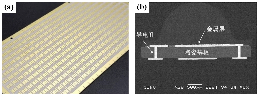
The specific features include :1) The use of semiconductor micromachining technology, ceramic substrate on the metal line is more fine, so DPC substrate is very suitable for the alignment of high precision microelectronics device packaging; 2) The vertical interconnection between the upper and lower surfaces of the ceramic substrate is realized by using laser drilling and electroplating filling technology, which can realize three-dimensional packaging and integration of electronic devices and reduce the device volume, as shown in Figure 2; 3) The thickness of the line layer is controlled by electroplating (usually 50-800μm), and the surface roughness of the line layer is reduced by grinding to meet the requirements of high temperature and large current device packaging; 4) Low temperature preparation process (below 300°C), to avoid the adverse effect of high temperature on the substrate material and metal line layer, but also reduce the production cost.
In summary, THE DPC substrate has the characteristics of high graphic accuracy, vertical interconnection and so on, which is a real ceramic circuit board. But DPC substrate also has some shortcomings :1) the metal circuit layer is prepared by electroplating process, which causes serious environmental pollution; 2) The electroplating growth rate is low which is difficult to meet the packaging requirements of high current power devices. At present, DPC ceramic substrate is mainly used for high-power LED packaging, and the manufacturers are mainly concentrated in Taiwan, China. However, mass production has begun in the Mainland since 2015.

Figure 2. (a) DPC ceramic substrate products and (b) sectional diagram
The key to the preparation of electroplated ceramic substrate
The bonding strength of metal circuit layer and ceramic substrate is the key to the reliability of DPC ceramic substrate. In order to reduce the interfacial stress, it is necessary to increase the transition layer between the copper layer and the ceramic layer to improve the interfacial bonding strength due to the large difference of thermal expansion coefficient between the metal and the ceramic layer. Because the bonding force between the transition layer and the ceramics is mainly diffusion adhesion and chemical bond, the metals with high activity and good diffusion such as Ti, Cr and Ni are often selected as the transition layer (and also as the seed layer of electroplating). Plasma cleaning of ceramic substrate can greatly improve the bonding strength between ceramic substrate and metal film, mainly because 1) the pollutants on the surface of ceramic substrate are removed by ion beam; 2) Ceramic substrate is bombarded by ion beam and produces suspension bond, which is more closely combined with metal atoms.
Electroplating hole filling is also the key technology of preparing DPC ceramic substrate. At present, DPC substrate electroplating hole filling mostly uses pulse power, its technical advantages include :1) easy to fill through hole, reduce the hole coating defects; 2) The surface coating has compact structure and uniform thickness; 3) Higher current density can be used for electroplating to improve deposition efficiency. Due to the high cost of pulse electroplating, the new type of DC electroplating has been paid more attention in recent years. By optimizing the plating solution formulation (including leveling agent, inhibitor, etc.), the efficient filling of blind hole or through hole can be realized.
Application and analysis of ceramic substrate
01
IGBT packaging
With high input impedance, fast switching speed, low on-state current and high blocking voltage, insulated gate bipolar transistor has become the mainstream of power semiconductor devices. Its applications are as small as variable frequency air conditioning, silent refrigerator, washing machine, induction cooker, microwave oven and other household appliances, and as large as electric locomotive traction system. Because of IGBT high output power, heat, so for IGBT packaging, heat dissipation is the key. At present IGBT packaging mainly uses DBC ceramic substrate, the reason is that DBC has a large metal layer thickness, high bonding strength (good thermal impact) and other characteristics.
02
LD packaging
Laser diode (LD), also known as semiconductor laser, is a photoelectric device based on the principle of stimulated radiation of semiconductor materials, has the characteristics of small volume, long life, easy to pump and integration. Widely used in laser communication, optical storage, optical gyro, laser printing, ranging and radar and other fields. The temperature has a great relationship with the output power of the semiconductor laser. Heat dissipation is key to LD encapsulation. Due to the high current density and heat flux of LD devices, ceramic substrate is the preferred heat sink material for LD packaging.
03
LED packaging
Throughout the development of LED technology, the power density continues to improve, the requirements for heat dissipation are becoming higher and higher. Due to the high insulation, high thermal conductivity and heat resistance, low expansion and other characteristics of ceramics, especially the use of through hole interconnection technology, can effectively meet the LED flip-chip, eutectic, COB(chip on board), CSP(chip scale packaging), WLP (wafer packaging) packaging requirements, suitable for medium and high power LED packaging.
04
Photovoltaic (PV) module package
Photovoltaic power generation is based on the principle of photovoltaic effect, using solar cells to directly convert sunlight into electricity. As the focusing effect leads to the increase of sunlight density and chip temperature, ceramic substrate must be used to strengthen heat dissipation. In practical applications, the metal layer on the surface of the ceramic substrate is connected with the chip and the heat sink respectively through the thermal interface material (TIM), and the heat is rapidly transmitted to the metal heat sink through the ceramic substrate, which effectively improves the photoelectric conversion efficiency and reliability of the system.
For more details on electroplated ceramic substrates, please look forward to the "2020 third New Ceramic Technology and Industry Summit", which will be held by China Powder network on October 29-30, 2020 in Wuxi. At that time, Professor Chen Mingxiang of Huazhong University of Science and Technology, founder of Wuhan Lizhida Technology will bring a report entitled "electroplated ceramic substrate (DPC) technology research and development and application" to answer your questions.
Expert introduction
Chen Mingxiang: Professor/doctoral supervisor of School of Mechanical Engineering, Huazhong University of Science and Technology, researcher of Wuhan National Research Center of Optoelectronics, Chair Professor of Guangdong Pearl River Scholars. He graduated from School of Materials, Wuhan University of Technology with bachelor's and master's degree. He graduated from School of Optoelectronics, Huazhong University of Science and Technology with doctor's degree. He is a postdoctoral fellow at the Packaging Research Center of Georgia Institute of Technology. Mainly engaged in advanced electronic packaging and micro/nano manufacturing technology research, including power device packaging (such as LED, LD, IGBT, CPV, etc.), low temperature bonding, system integration technology, etc. His research projects include national Natural Science Foundation of China, National Key RESEARCH and Development Program, "863 Program" and Support Program of The Ministry of Science and Technology, Key project of Assembly Pre-research Fund, Key project of Industry-University-Research Cooperation in Guangdong Province, Key project of Science and Technology Innovation in Hubei Province, and major project of Transformation of Scientific and technological Achievements in Wuhan city, etc. He has published more than 60 academic papers (more than 40 of which were indexed by SCI), and has been granted more than 20 invention patents (DPC ceramic substrate technology has been industrialized through patent transfer). He has won the Second Prize of National Technological Invention (2016), the first prize of Technological Invention of the Ministry of Education (2015), "3551 Optical Valley Talent" of Wuhan East Lake High-tech Zone (2012), and the Third Prize of Science and Technology of Guangdong Province (2010).
References:
Qin D C. Research status and development trend of surface metallization of ceramic substrate
Chen Ming-xiang. Advances in technology and application of ceramic substrates for power electronic packaging
Chen Ming xiang. Ceramic substrate for electronic packaging
Forum social routine many

